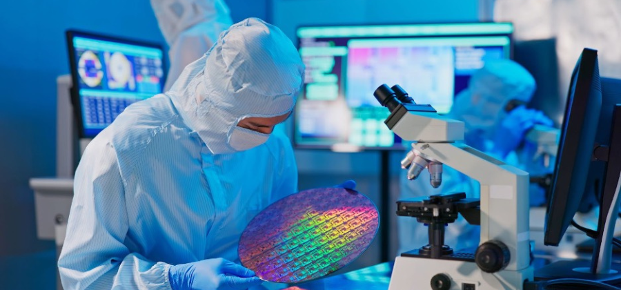
The semiconductor industry is currently drowning in data and starving for answers. Every wafer produced contains millions of die-level measurements that reveal exactly where processes fail, which tools are drifting, and why yields are stagnating. The pain is that most fabs are still reading this story backwards, after the damage is done, through manual inspection workflows designed for a world that no longer exists.
That needs to stop.
We’re entering a phase of semiconductor manufacturing where proactive yield management is no longer optional but a competitive necessity. With die shrinks pushing deeper into sub-3nm territory (TSMC‘s 3nm monthly capacity is rapidly approaching 200,000 wafers!), the margin for undetected process excursions has essentially vanished. Edge exclusion zones, lithography non-uniformities, and Chemical Vapor Deposition (CVD) ring effects, all these aren’t random noise. They are deterministic, spatially coherent signatures that repeat across wafers, across lots, and across time. And they are perfectly visible, if you know where and how to look!
The zone is the signal
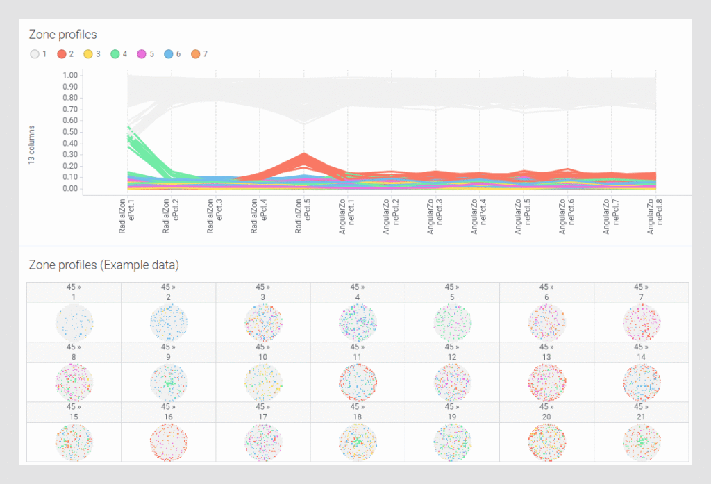
This is why wafer zone analysis represents one of the most underutilized methodologies in advanced yield engineering. The concept is simple: divide the wafer into radial zones, concentric rings from center to edge, and angular zones pie-slice sectors around the circumference. Suddenly, what looked like a scattered defect cloud resolves into a crisp fingerprint. A high-density outer ring tells you edge bead removal is off. Consistent angular anomalies at a fixed clock position point straight at a chuck tilt or shower-head asymmetry. Batch-to-batch zone profile divergence highlights a consumable degradation before your Statistical Process Control (SPC) charts report any issue.
Visual industrial analytics tools like Spotfire that offer support for wafer zone analysis are rapidly closing the gap. By automating the segmentation of spatial data into configurable zones, engineers can now compare profiles across wafers and lots within a single application. This moves root cause analysis directly into the hands of process and equipment engineers—eliminating the need for scripting, manual data exports, or waiting days for specialized analysis requests.
The signal has always been there; we now have the tools to read it fluently and at scale.
The real advantage: speed to root cause
In a world where a single photolithography tool can process 200+ wafers per day, every hour of undetected systematic excursion translates directly to scrapped silicon and margin erosion. The engineers I’ve seen succeed in high-volume manufacturing share one trait: They’ve made root cause analysis a reflex, not a project. Zone-based spatial analytics is how you build that reflex into your organization’s standard operating workflow.
When your team can identify a recurring outer-ring yield signature, link it to a specific etch chamber through zone profile correlation, and initiate a preventive maintenance intervention, all within the same shift, the pattern emerges: You’re not just doing better analysis, you’re operating a fundamentally different class of factory.
The conversation the industry needs to have
Here’s the uncomfortable question every VP of Manufacturing or Fab Manager should be asking right now: How long does it take your organization to identify a systematic yield issue and trace it to a root cause? Whether the answer is days or weeks, if the exact timeframe is unknown, that is an answer in itself.
The capability to resolve these issues in hours already exists. The data is already being generated. The bottleneck is not sensors, not compute, not even talent; it’s the absence of purpose-built analytical workflows that make spatial pattern intelligence accessible at the point of decision.
Wafer zone analysis isn’t a feature. It’s a capability your competitors are already building into their operations. The window to make it a differentiator rather than a catch-up initiative is narrowing.
Your wafer is talking. It’s time to listen. Find out more.